Capes
Previous chapters of this book show a variety of ways to interface BeagleBone Black to the physical world by using a breadboard and wiring to the +P8+ and +P9+ headers. This is a great approach because it’s easy to modify your circuit to debug it or try new things. At some point, though, you might want a more permanent solution, either because you need to move the Bone and you don’t want wires coming loose, or because you want to share your hardware with the masses.
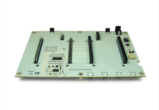
You can easily expand the functionality of the Bone by adding a cape. A cape is simply a board–often a printed circuit board (PCB) that connects to the +P8+ and +P9+ headers and follows a few standard pin usages. You can stack up to four capes onto the Bone. Capes can range in size from Bone-sized (Using a 128 x 128-Pixel LCD Cape) to much larger than the Bone (Using a Seven-Inch LCD Cape).
This chapter shows how to attach a couple of capes, move your design to a protoboard, then to a PCB, and finally on to mass production.
Using a Seven-Inch LCD Cape
Problem
You want to display the Bone’s desktop on a portable LCD.
Solution
Note
#TODO# The 4D Systems LCD capes would make a better example. CircuitCo is out of business.
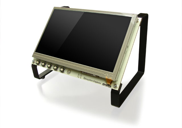
A number of LCD capes are built for the Bone, ranging in size from three to seven inches. This recipe attaches a seven-inch BeagleBone LCD7 from CircuitCo (shown in 7” LCD) to the Bone.
7” LCD
Note
Seven-inch LCD from CircuitCo, 7” LCD was originally posted by CircuitCo at http://elinux.org/File:BeagleBone-LCD7-Front.jpg under a Creative Commons Attribution-ShareAlike 3.0 Unported License.
To make this recipe, you will need:
Seven-inch LCD cape
A 5 V power supply
Just attach the Bone to the back of the LCD, making sure pin 1 of P9 lines up with pin 1 of +P9+ on the LCD. Apply a 5 V power supply, and the desktop will appear on your LCD, as shown in Seven-inch LCD desktop.
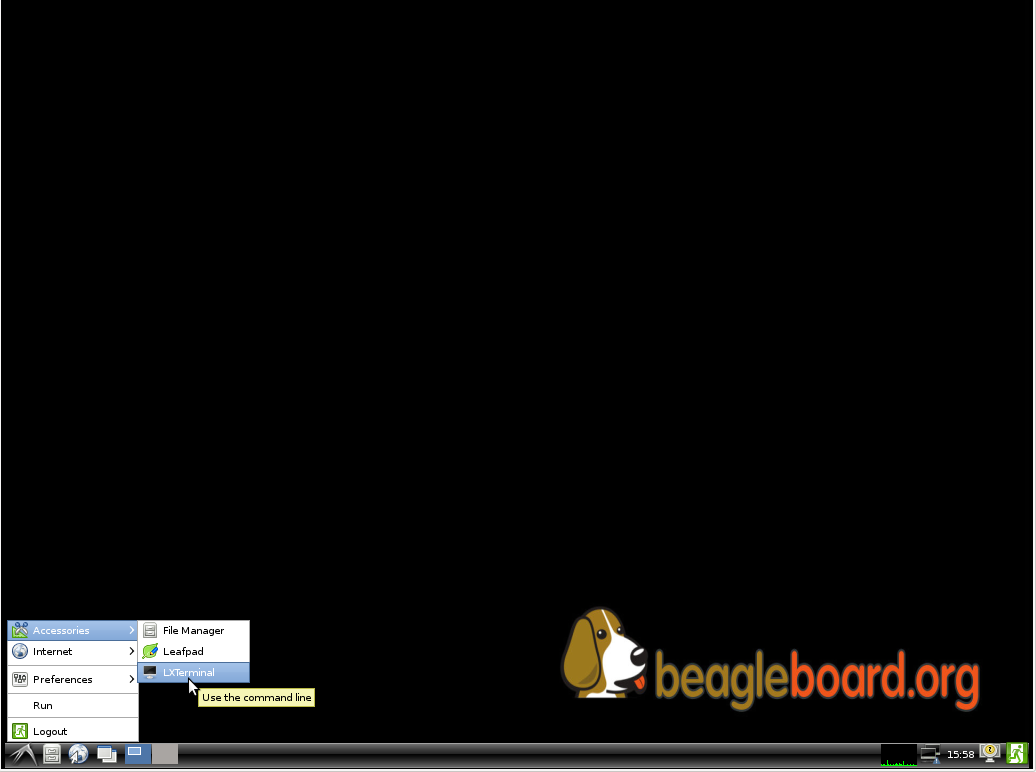
Fig. 246 Seven-inch LCD desktop
Attach a USB keyboard and mouse, and you have a portable Bone. Wireless keyboard and mouse combinations make a nice solution to avoid the need to add a USB hub.
Using a 128 x 128-Pixel LCD Cape
Problem
You want to use a small LCD to display things other than the desktop.
Solution
The MiniDisplay is a 128 x 128 full-color LCD cape that just fits on the Bone, as shown in MiniDisplay 128 x 128-pixel LCD from CircuitCo.
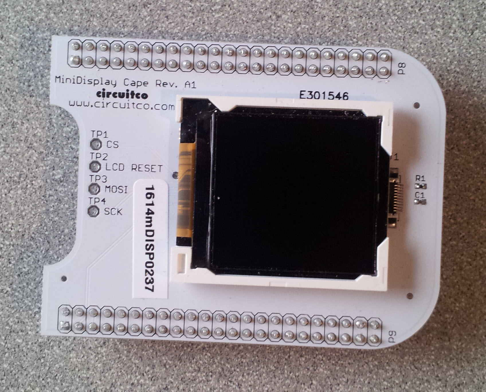
Fig. 247 MiniDisplay 128 x 128-pixel LCD from CircuitCo
To make this recipe, you will need:
MiniDisplay LCD cape
Attach to the Bone and apply power. Then run the following commands:
# From http://elinux.org/CircuitCo:MiniDisplay_Cape
# Datasheet:
# https://www.crystalfontz.com/products/document/3277/ST7735_V2.1_20100505.pdf
bone$ wget http://elinux.org/images/e/e4/Minidisplay-example.tar.gz
bone$ tar zmxvf Minidisplay-example.tar.gz
bone$ cd minidisplay-example
bone$ make
bone$ ./minidisplay-test
Unable to initialize SPI: No such file or directory
Aborted
Warning
You might get a compiler warning, but the code should run fine.
The MiniDisplay uses the Serial Peripheral Interface (SPI) interface, and it’s not initialized. The manufacturer’s website suggests enabling SPI0 by using the following commands:
bone$ export SLOTS=/sys/devices/bone_capemgr.*/slots
bone$ echo BB-SPIDEV0 > $SLOTS
Hmmm, something isn’t working here. Here’s how to see what happened:
Here’s how to see what’s already configured:
You can unconfigure it by using the following commands:
bone$ echo -10 > $SLOTS
bone$ cat $SLOTS
0: 54:PF---
1: 55:PF---
2: 56:PF---
3: 57:PF---
4: ff:P-O-L Bone-LT-eMMC-2G,00A0,Texas Instrument,BB-BONE-EMMC-2G
5: ff:P-O-L Bone-Black-HDMI,00A0,Texas Instrument,BB-BONELT-HDMI
7: ff:P-O-L Override Board Name,00A0,Override Manuf,bspm_P9_42_27
8: ff:P-O-L Override Board Name,00A0,Override Manuf,bspm_P9_41_27
9: ff:P-O-L Override Board Name,00A0,Override Manuf,am33xx_pwm
Now P9_21 is free for the MiniDisplay to use.
Note
In future Bone images, all of the pins will already be allocated as part of the main device tree using runtime pinmux helpers and configured at runtime using the config-pin utility. This would eliminate the need for device tree overlays in most cases.
Now, configure it for the MiniDisplay and run a test:
bone$ echo BB-SPIDEV0 > $SLOTS
bone$ ./minidisplay-test
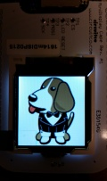
You then see Boris, as shown in Mini display Boris.
Mini display Boris
Note
MiniDisplay showing Boris, Mini display Boris was originally posted by David Anders at http://elinux.org/File:Minidisplay-boris.jpg under a Creative Commons Attribution-ShareAlike 3.0 Unported License.
Connecting Multiple Capes
Problem
You want to use more than one cape at a time.
Solution
First, look at each cape that you want to stack mechanically. Are they all using stacking headers like the ones shown in Stacking headers? No more than one should be using non-stacking headers.

Fig. 248 Stacking headers
Note that larger LCD panels might provide expansion headers, such as the ones shown in LCD Backside, rather than the stacking headers, and that those can also be used for adding additional capes.
LCD Backside
Note
Back side of LCD7 cape, LCD Backside was originally posted by CircuitCo at http://elinux.org/File:BeagleBone-LCD-Backside.jpg under a Creative Commons Attribution-ShareAlike 3.0 Unported License.
Note
#TODO# One of the 4D Systems LCD capes would make a better example for an LCD cape. The CircuitCo cape is no longer available.
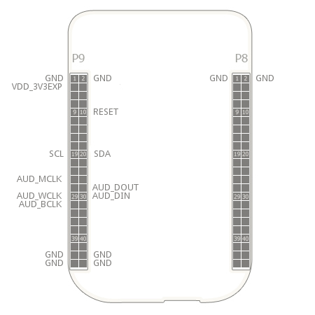
Next, take a note of each pin utilized by each cape. The BeagleBone Capes catalog provides a graphical representation for the pin usage of most capes, as shown in Audio cape pins for the Circuitco Audio Cape.
Note
#TODO# Bela would make a better example for an audio cape. The CircuitCo cape is no longer available.
Audio cape pins
Note
Pins utilized by CircuitCo Audio Cape, Audio cape pins was originally posted by Djackson at http://elinux.org/File:Audio_pins_revb.png under a Creative Commons Attribution-ShareAlike 3.0 Unported License.
In most cases, the same pin should never be used on two different capes, though in some cases, pins can be shared. Here are some exceptions:
- GND
The ground (GND) pins should be shared between the capes, and there’s no need to worry about consumed resources on those pins.
- VDD_3V3
The 3.3 V power supply (VDD_3V3) pins can be shared by all capes to supply power, but the total combined consumption of all the capes should be less than 500 mA (250 mA per VDD_3V3 pin).
- VDD_5V
The 5.0 V power supply (VDD_5V) pins can be shared by all capes to supply power, but the total combined consumption of all the capes should be less than 2 A (1 A per +VD*_5V+ p*n). It is possible for one, and only one, of the capes to _provide_ power to this pin rather than consume it, and it should provide at least 3 A to ensure proper system function. Note that when no voltage is applied to the DC connector, nor from a cape, these pins will not be powered, even if power is provided via USB.
- SYS_5V
The regulated 5.0 V power supply (SYS_5V) pins can be shared by all capes to supply power, but the total combined consumption of all the capes should be less than 500 mA (250 mA per SYS_5V pin).
- VADC and AGND
The ADC reference voltage pins can be shared by all capes.
- I2C2_SCL and I2C2_SDA
I2C is a shared bus, and the I2C2_SCL and I2C2_SDA pins default to having this bus enabled for use by cape expansion ID EEPROMs.
Moving from a Breadboard to a Protoboard
Problem
You have your circuit working fine on the breadboard, but you want a more reliable solution.
Solution
Solder your components to a protoboard.
To make this recipe, you will need:
Protoboard
Soldering iron
Your other components
Many places make premade circuit boards that are laid out like the breadboard we have been using. Beaglebread shows the BeagleBone Breadboard, which is just one protoboard option.
Beaglebread
Note
This was originally posted by William Traynor at http://elinux.org/File:BeagleBone-Breadboard.jpg under a Creative Commons Attribution-ShareAlike 3.0 Unported License
You just solder your parts on the protoboard as you had them on the breadboard.
Creating a Prototype Schematic
Problem
You’ve wired up a circuit on a breadboard. How do you turn that prototype into a schematic others can read and that you can import into other design tools?
Solution
In Fritzing tips, we introduced Fritzing as a useful tool for drawing block diagrams. Fritzing can also do circuit schematics and printed-circuit layout. For example, A simple robot controller diagram (quickBot.fzz) shows a block diagram for a simple robot controller (quickBot.fzz is the name of the Fritzing file used to create the diagram).
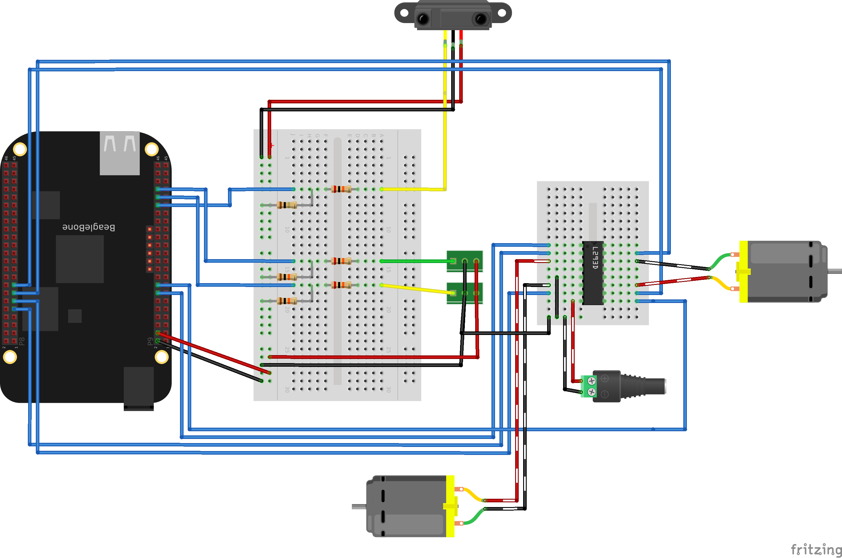
Fig. 249 A simple robot controller diagram (quickBot.fzz)
The controller has an H-bridge to drive two DC motors (Controlling the Speed and Direction of a DC Motor), an IR range sensor, and two headers for attaching analog encoders for the motors. Both the IR sensor and the encoders have analog outputs that exceed 1.8 V, so each is run through a voltage divider (two resistors) to scale the voltage to the correct range (see Reading a Distance Sensor (Variable Pulse Width Sensor) for a voltage divider example).
Automatically generated schematic shows the schematic automatically generated by Fritzing. It’s a mess. It’s up to you to fix it.
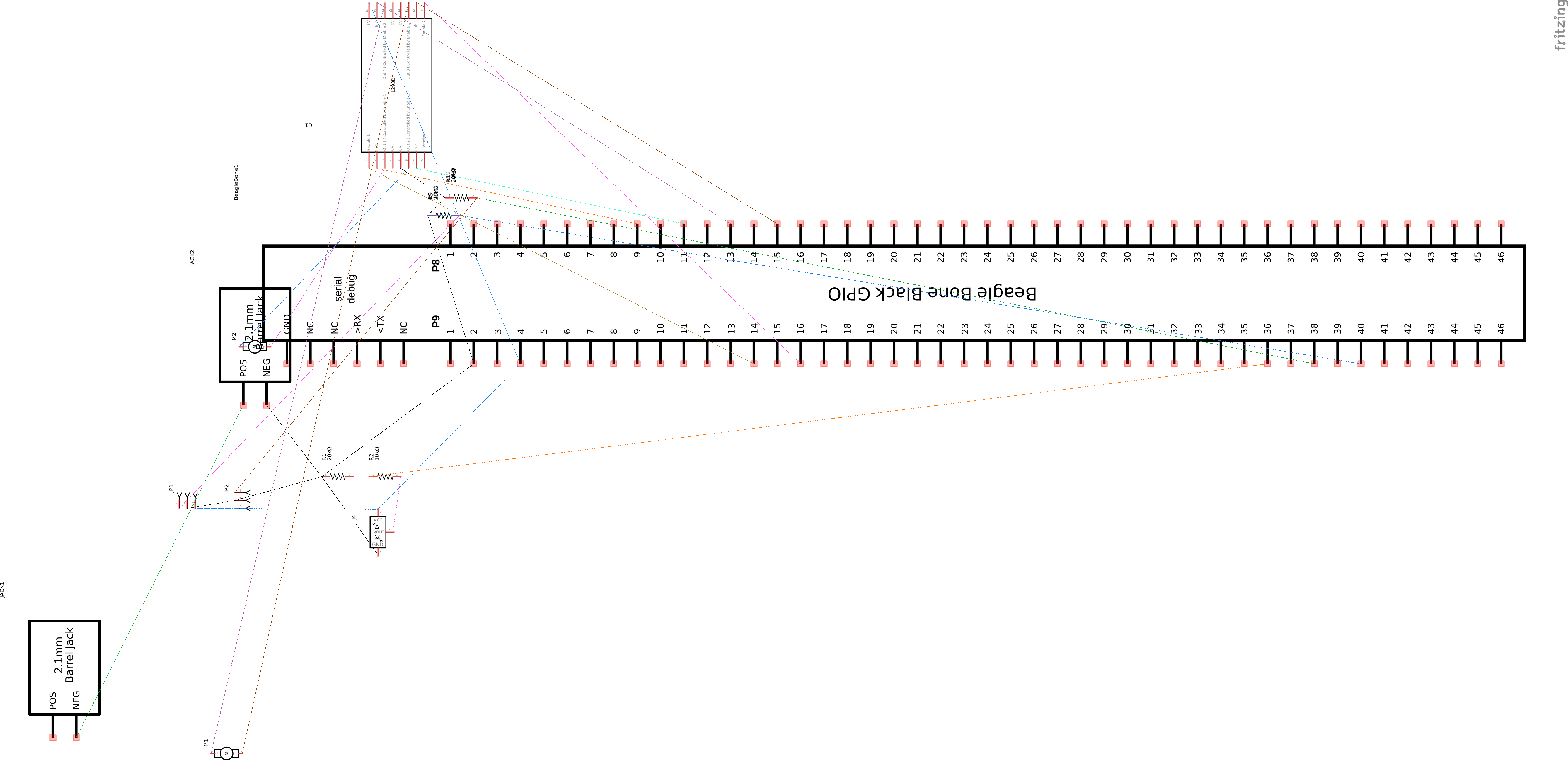
Fig. 250 Automatically generated schematic
Cleaned-up schematic shows my cleaned-up schematic. I did it by moving the parts around until it looked better.
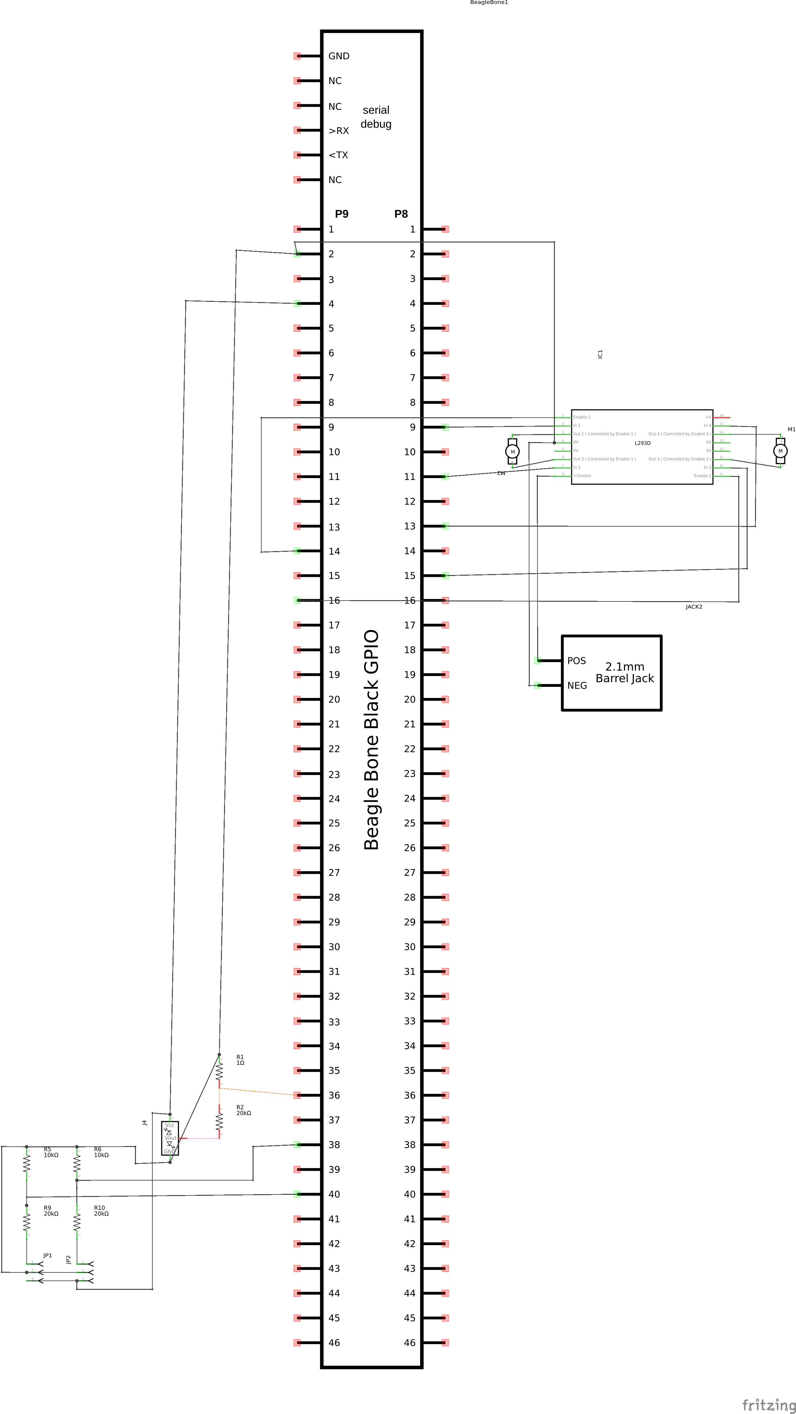
Fig. 251 Cleaned-up schematic
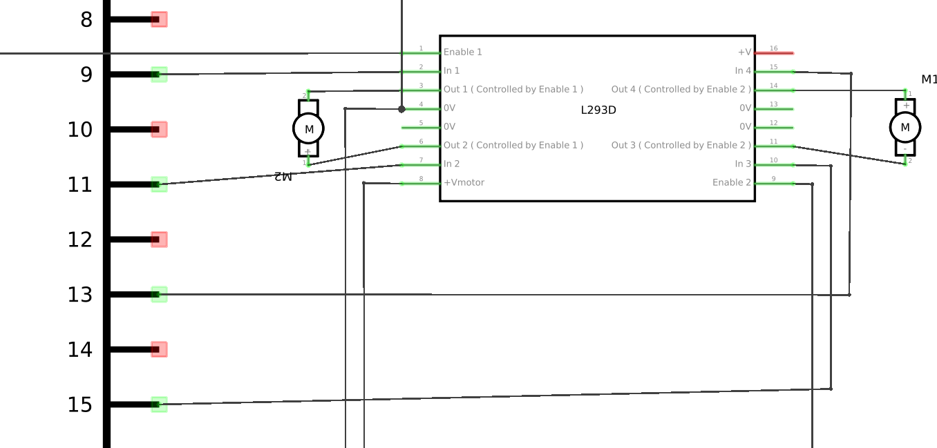
Fig. 252 Zoomed-in schematic
You might find that you want to create your design in a more advanced design tool, perhaps because it has the library components you desire, it integrates better with other tools you are using, or it has some other feature (such as simulation) of which you’d like to take advantage.
Verifying Your Cape Design
Problem
You’ve got a design. How do you quickly verify that it works?
Solution
To make this recipe, you will need:
An oscilloscope
Break down your design into functional subcomponents and write tests for each. Use components you already know are working, such as the onboard LEDs, to display the test status with the code in Testing the quickBot motors interface (quickBot_motor_test.js).
Testing the quickBot motors interface (quickBot_motor_test.js)
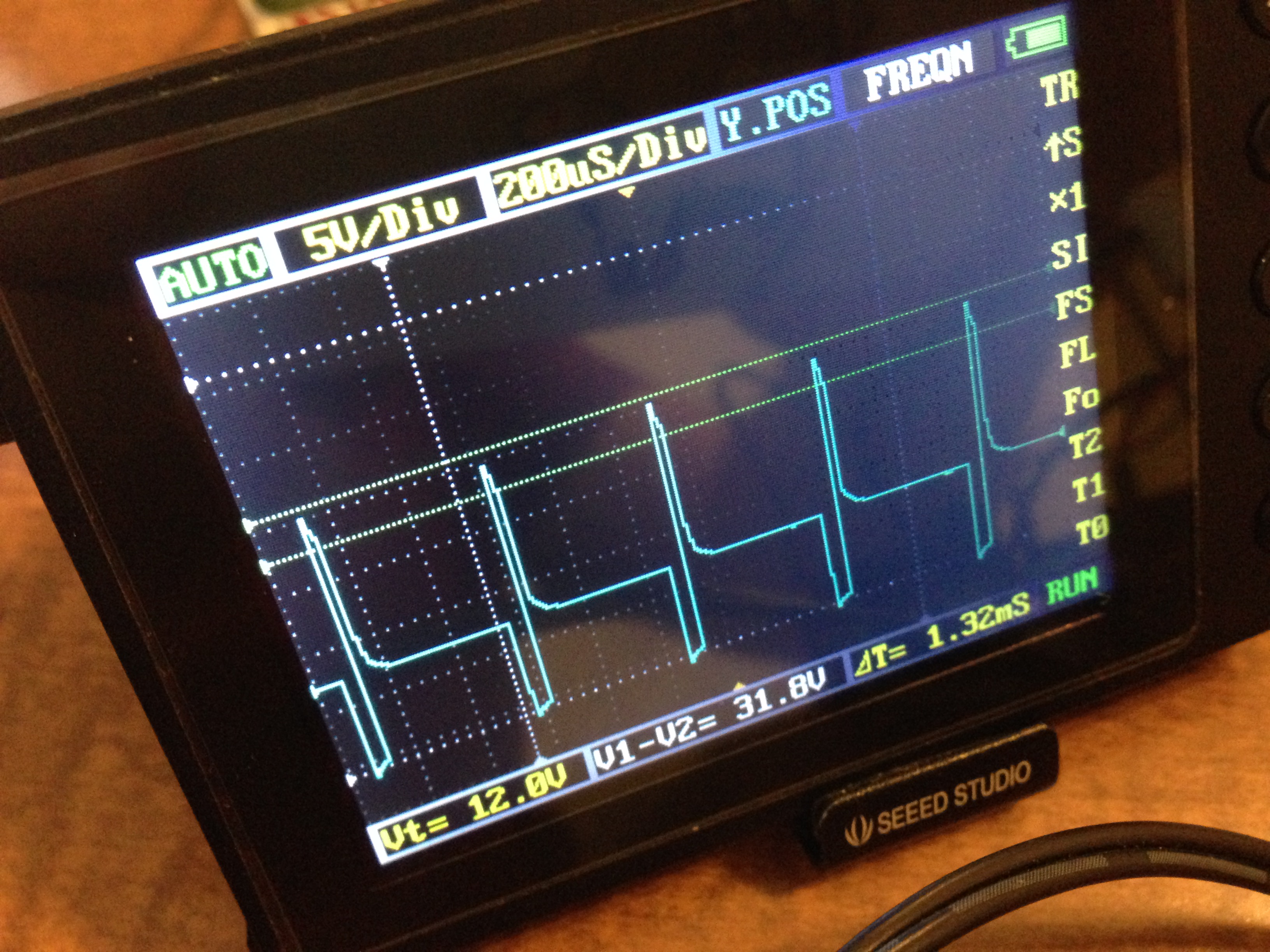
Fig. 253 quickBot motor test showing kickback
Using the solution in Basics, you can untether from your coding station to test your design at your lab workbench, as shown in quickBot motor test code under scope.
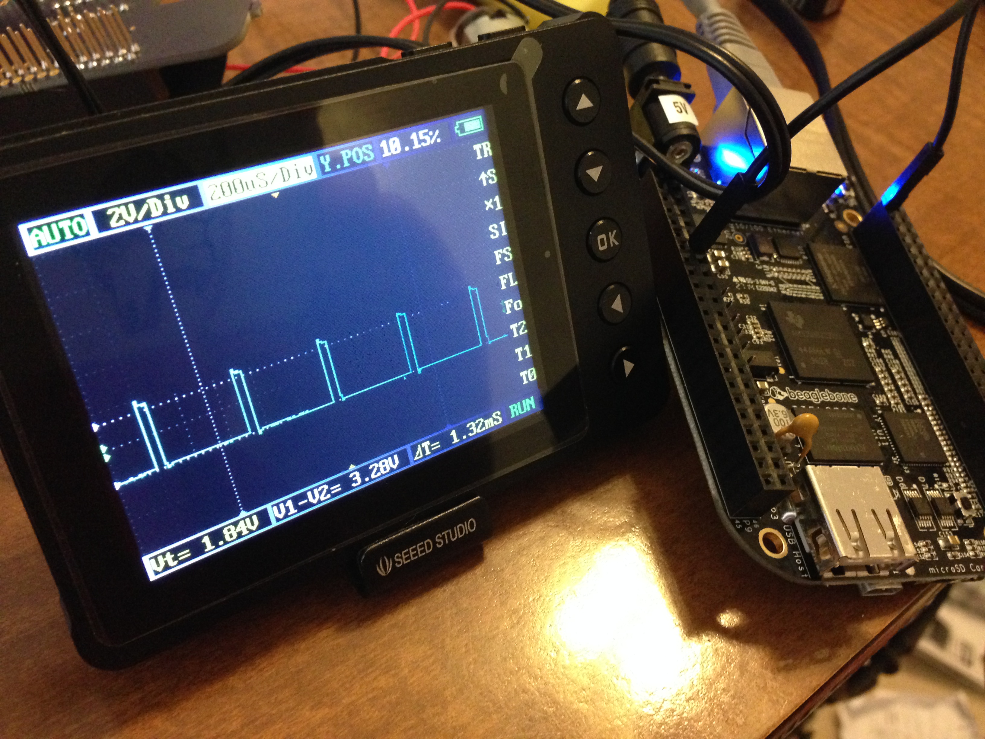
Fig. 254 quickBot motor test code under scope
SparkFun provides a useful guide to using an oscilloscope. You might want to check it out if you’ve never used an oscilloscope before. Looking at the stimulus you’ll generate before you connect up your hardware will help you avoid surprises.
Laying Out Your Cape PCB
Problem
You’ve generated a diagram and schematic for your circuit and verified that they are correct. How do you create a PCB?
Solution
If you’ve been using Fritzing, all you need to do is click the PCB tab, and there’s your board. Well, almost. Much like the schematic view shown in Creating a Prototype Schematic, you need to do some layout work before it’s actually usable. I just moved the components around until they seemed to be grouped logically and then clicked the Autoroute button. After a minute or two of trying various layouts, Fritzing picked the one it determined to be the best. Simple robot PCB shows the results.
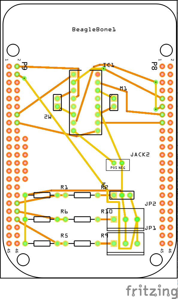
Fig. 255 Simple robot PCB
The Fritzing pre-fab web page has a few helpful hints, including checking the widths of all your traces and cleaning up any questionable routing created by the autorouter.
The PCB in Simple robot PCB is a two-sided board. One color (or shade of gray in the printed book) represents traces on one side of the board, and the other color (or shade of gray) is the other side. Sometimes, you’ll see a trace come to a small circle and then change colors. This is where it is switching sides of the board through what’s called a _via_. One of the goals of PCB design is to minimize the number of vias.
Simple robot PCB wasn’t my first try or my last. My approach was to see what was needed to hook where and move the components around to make it easier for the autorouter to carry out its job.
Note
There are entire books and websites dedicated to creating PCB layouts. Look around and see what you can find. SparkFun’s guide to making PCBs is particularly useful.
Customizing the Board Outline
One challenge that slipped my first pass review was the board outline. The part we installed in Fritzing tips is meant to represent BeagleBone Black, not a cape, so the outline doesn’t have the notch cut out of it for the Ethernet connector.
The Fritzing custom PCB outline page describes how to create and use a custom board outline. Although it is possible to use a drawing tool like Inkscape, I chose to use the SVG path command directly to create Outline SVG for BeagleBone cape (beaglebone_cape_boardoutline.svg).
Outline SVG for BeagleBone cape (beaglebone_cape_boardoutline.svg)
The measurements are taken from the BeagleBone Black Mechanical section of the BeagleBone Black System Reference Manual, as shown in Cape dimensions.
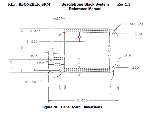
Fig. 256 Cape dimensions
You can observe the rendered output of Outline SVG for BeagleBone cape (beaglebone_cape_boardoutline.svg) quickly by opening the file in a web browser, as shown in Rendered cape outline in Chrome.
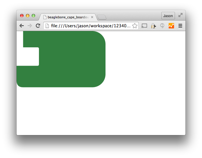
Fig. 257 Rendered cape outline in Chrome
Fritzing tips
After you have the SVG outline, you’ll need to select the PCB in Fritzing and select a custom shape in the Inspector box. Begin with the original background, as shown in PCB with original board, without notch for Ethernet connector.
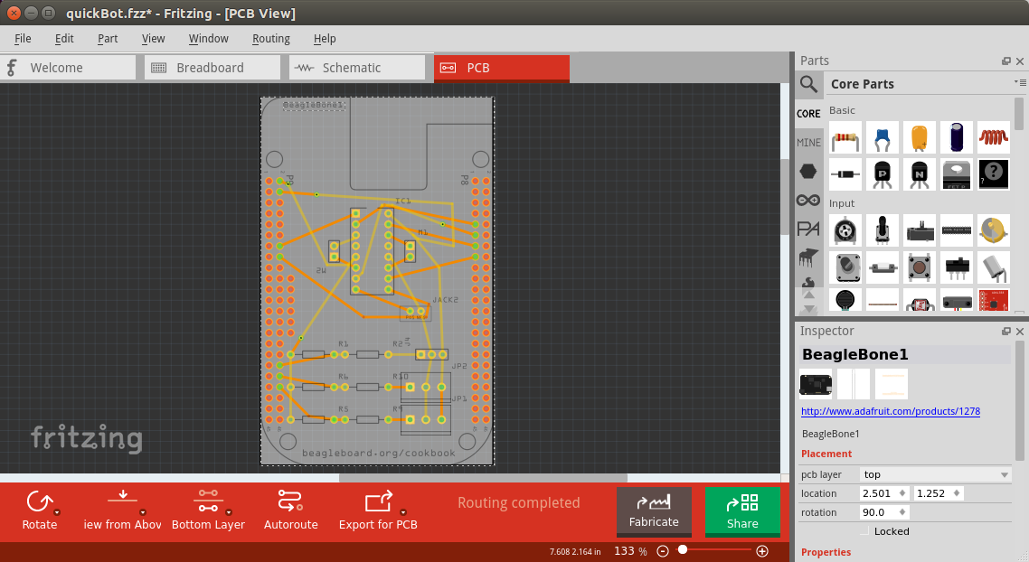
Fig. 258 PCB with original board, without notch for Ethernet connector
Hide all but the Board Layer (PCB with all but the Board Layer hidden).
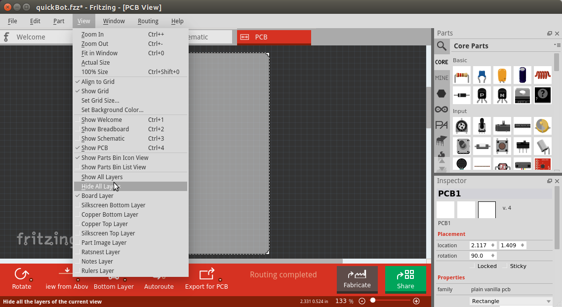
Fig. 259 PCB with all but the Board Layer hidden
Select the PCB1 object and then, in the Inspector pane, scroll down to the “load image file” button (Clicking :load image file: with PCB1 selected).
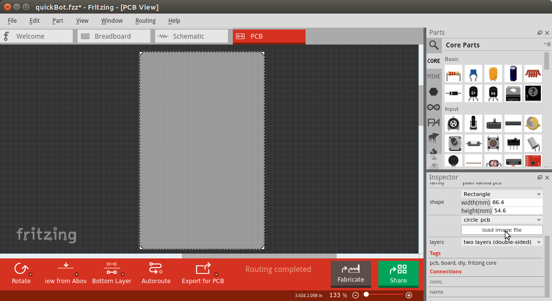
Fig. 260 Clicking :load image file: with PCB1 selected
Navigate to the beaglebone_cape_boardoutline.svg file created in Outline SVG for BeagleBone cape (beaglebone_cape_boardoutline.svg), as shown in Selecting the .svg file.
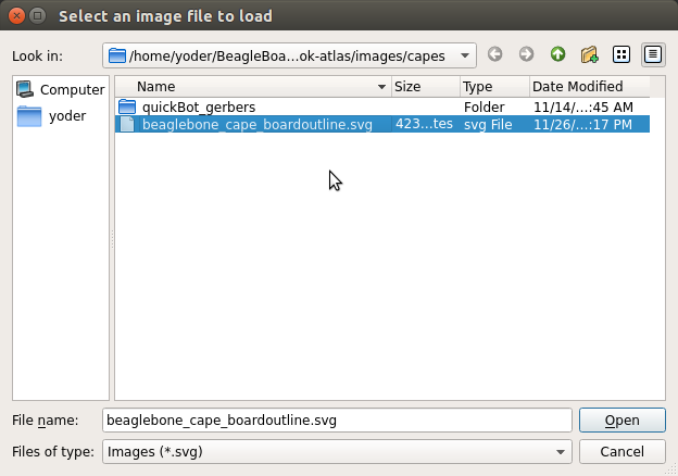
Fig. 261 Selecting the .svg file
Turn on the other layers and line up the Board Layer with the rest of the PCB, as shown in PCB Inspector.
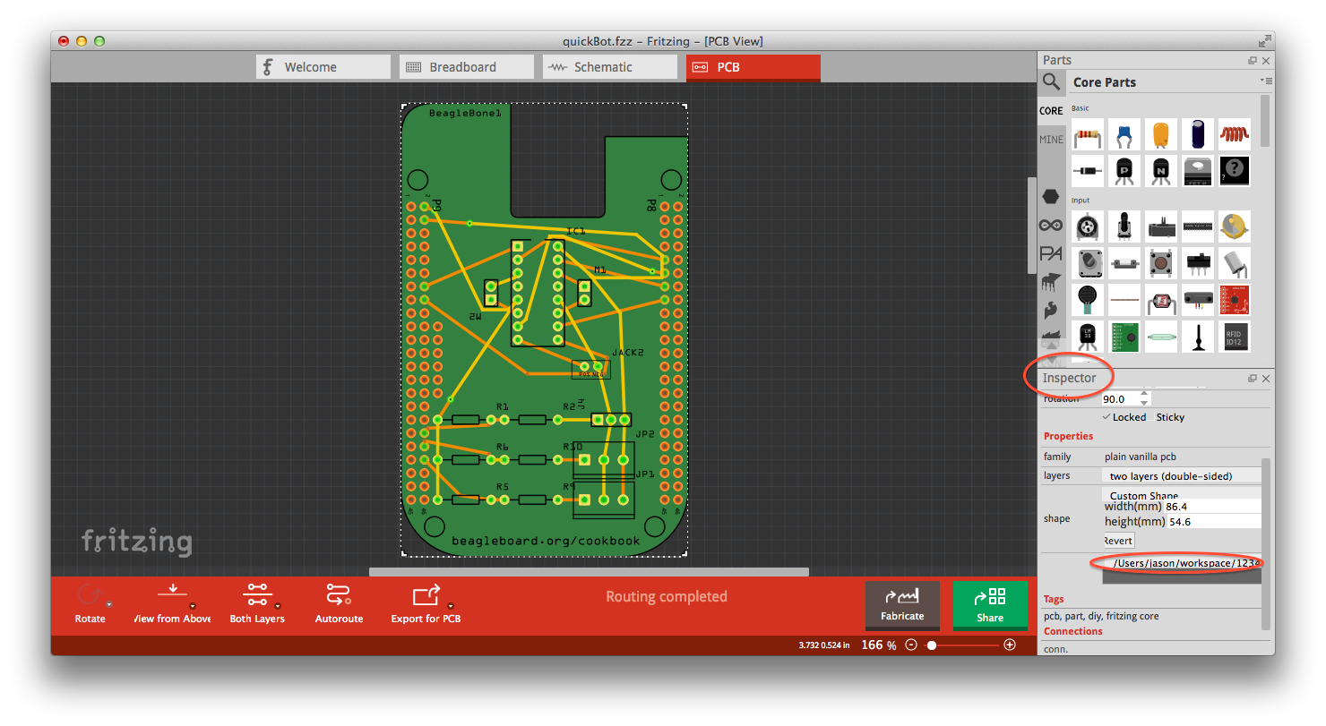
Fig. 262 PCB Inspector
Now, you can save your file and send it off to be made, as described in Producing a Prototype.
PCB Design Alternatives
There are other free PCB design programs. Here are a few.
TO PROD: The headings I’ve marked as bold lines really should be subheadings of “PCB Design Alternatives,” but AsciiDoc won’t let me go that deep (to the level). Is what I’ve done the best solution, or is there a way to create another heading level?
EAGLE
Eagle PCB and DesignSpark PCB are two popular design programs. Many capes (and other PCBs) are designed with Eagle PCB, and the files are available. For example, the MiniDisplay cape (Using a 128 x 128-Pixel LCD Cape) has the schematic shown in Schematic for the MiniDisplay cape and PCB shown in PCB for MiniDisplay cape.
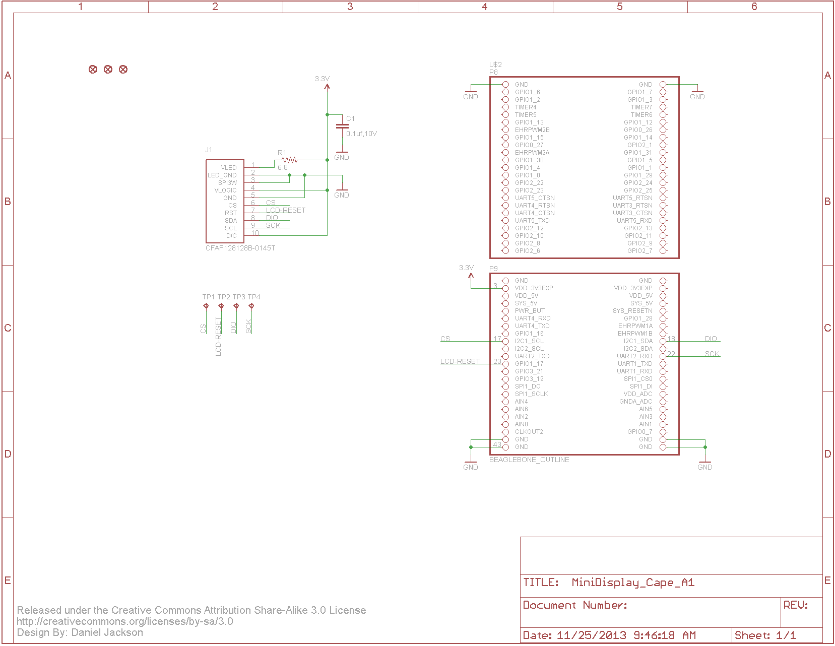
Fig. 263 Schematic for the MiniDisplay cape
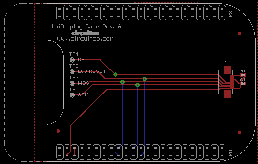
Fig. 264 PCB for MiniDisplay cape
A good starting point is to take the PCB layout for the MiniDisplay and edit it for your project. The connectors for +P8+ and +P9+ are already in place and ready to go.
Eagle PCB is a powerful system with many good tutorials online. The free version runs on Windows, Mac, and Linux, but it has three limitations:
The usable board area is limited to 100 x 80 mm (4 x 3.2 inches).
You can use only two signal layers (Top and Bottom).
The schematic editor can create only one sheet.
You can install Eagle PCB on your Linux host by using the following command:
host$ sudo apt install eagle
Reading package lists... Done
Building dependency tree
Reading state information... Done
...
Setting up eagle (6.5.0-1) ...
Processing triggers for libc-bin (2.19-0ubuntu6.4) ...
host$ eagle
You’ll see the startup screen shown in Eagle PCB startup screen.
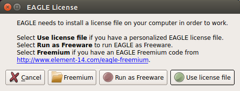
Fig. 265 Eagle PCB startup screen
Click “Run as Freeware.” When my Eagle started, it said it needed to be updated. To update on Linux, follow the link provided by Eagle and download eagle-lin-7.2.0.run (or whatever version is current.). Then run the following commands:
host$ chmod +x eagle-lin-7.2.0.run
host$ ./eagle-lin-7.2.0.run
A series of screens will appear. Click Next. When you see a screen that looks like The Eagle installation destination directory, note the Destination Directory.
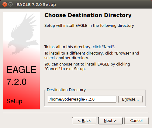
Fig. 266 The Eagle installation destination directory
Continue clicking Next until it’s installed. Then run the following commands (where ~/eagle-7.2.0 is the path you noted in The Eagle installation destination directory):
host$ cd /usr/bin
host$ sudo rm eagle
host$ sudo ln -s ~/eagle-7.2.0/bin/eagle .
host$ cd
host$ eagle
The ls command links eagle in /usr/bin, so you can run +eagle+ from any directory. After eagle starts, you’ll see the start screen shown in The Eagle start screen.
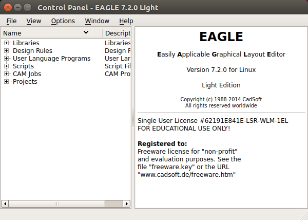
Fig. 267 The Eagle start screen
Ensure that the correct version number appears.
If you are moving a design from Fritzing to Eagle, see Migrating a Fritzing Schematic to Another Tool for tips on converting from one to the other.
DesignSpark PCB
The free DesignSpark PCB doesn’t have the same limitations as Eagle PCB, but it runs only on Windows. Also, it doesn’t seem to have the following of Eagle at this time.
Upverter
In addition to free solutions you run on your desktop, you can also work with a browser-based tool called Upverter. With Upverter, you can collaborate easily, editing your designs from anywhere on the Internet. It also provides many conversion options and a PCB fabrication service.
Note
Don’t confuse Upverter with Upconverter (Migrating a Fritzing Schematic to Another Tool). Though their names differ by only three letters, they differ greatly in what they do.
Kicad
Unlike the previously mentioned free (no-cost) solutions, Kicad is open source and provides some features beyond those of Fritzing. Notably, CircuitHub site (discussed in Putting Your Cape Design into Production) provides support for uploading Kicad designs.
Migrating a Fritzing Schematic to Another Tool
Problem
You created your schematic in Fritzing, but it doesn’t integrate with everything you need. How can you move the schematic to another tool?
Solution
Use the Upverter schematic-file-converter Python script. For example, suppose that you want to convert the Fritzing file for the diagram shown in A simple robot controller diagram (quickBot.fzz). First, install Upverter.
I found it necessary to install +libfreetype6+ and +freetype-py+ onto my system, but you might not need this first step:
host$ sudo apt install libfreetype6
Reading package lists... Done
Building dependency tree
Reading state information... Done
libfreetype6 is already the newest version.
0 upgraded, 0 newly installed, 0 to remove and 154 not upgraded.
host$ sudo pip install freetype-py
Downloading/unpacking freetype-py
Running setup.py egg_info for package freetype-py

Installing collected packages: freetype-py
Running setup.py install for freetype-py

Successfully installed freetype-py
Cleaning up...
Note
All these commands are being run on the Linux-based host computer, as shown by the +host$+ prompt. Log in as a normal user, not +root+.
Now, install the schematic-file-converter tool:
host$ git clone git@github.com:upverter/schematic-file-converter.git
Cloning into 'schematic-file-converter'...
remote: Counting objects: 22251, done.
remote: Total 22251 (delta 0), reused 0 (delta 0)
Receiving objects: 100% (22251/22251), 39.45 MiB | 7.28 MiB/s, done.
Resolving deltas: 100% (14761/14761), done.
Checking connectivity... done.
Checking out files: 100% (16880/16880), done.
host$ cd schematic-file-converter
host$ sudo python setup.py install
.
.
.
Extracting python_upconvert-0.8.9-py2.7.egg to \
    /usr/local/lib/python2.7/dist-packages
Adding python-upconvert 0.8.9 to easy-install.pth file

Installed /usr/local/lib/python2.7/dist-packages/python_upconvert-0.8.9-py2.7.egg
Processing dependencies for python-upconvert==0.8.9
Finished processing dependencies for python-upconvert==0.8.9
host$ cd ..
host$ python -m upconvert.upconverter -h
usage: upconverter.py [-h] [-i INPUT] [-f TYPE] [-o OUTPUT] [-t TYPE]
                    [-s SYMDIRS [SYMDIRS ...]] [--unsupported]
                    [--raise-errors] [--profile] [-v] [--formats]

optional arguments:
-h, --help            show this help message and exit
-i INPUT, --input INPUT
                        read INPUT file in
-f TYPE, --from TYPE  read input file as TYPE
-o OUTPUT, --output OUTPUT
                        write OUTPUT file out
-t TYPE, --to TYPE    write output file as TYPE
-s SYMDIRS [SYMDIRS ...], --sym-dirs SYMDIRS [SYMDIRS ...]
                        specify SYMDIRS to search for .sym files (for gEDA
                        only)
--unsupported         run with an unsupported python version
--raise-errors        show tracebacks for parsing and writing errors
--profile             collect profiling information
-v, --version         print version information and quit
--formats             print supported formats and quit
At the time of this writing, Upverter suppports the following file types:
File type |
Support |
openjson |
i/o |
kicad |
i/o |
geda |
i/o |
eagle |
i/o |
eaglexml |
i/o |
fritzing |
in only schematic only |
gerber |
i/o |
specctra |
i/o |
image |
out only |
ncdrill |
out only |
bom (csv) |
out only |
netlist (csv) |
out only |
After Upverter is installed, run the file (quickBot.fzz) that generated A simple robot controller diagram (quickBot.fzz) through Upverter:
host$ python -m upconvert.upconverter -i quickBot.fzz \
-f fritzing -o quickBot-eaglexml.sch -t eaglexml --unsupported
WARNING: RUNNING UNSUPPORTED VERSION OF PYTHON (2.7 > 2.6)
DEBUG:main:parsing quickBot.fzz in format fritzing
host$ ls -l
total 188
-rw-rw-r-- 1 ubuntu ubuntu  63914 Nov 25 19:47 quickBot-eaglexml.sch
-rw-r--r-- 1 ubuntu ubuntu 122193 Nov 25 19:43 quickBot.fzz
drwxrwxr-x 9 ubuntu ubuntu   4096 Nov 25 19:42 schematic-file-converter
Output of Upverter conversion shows the output of the conversion.
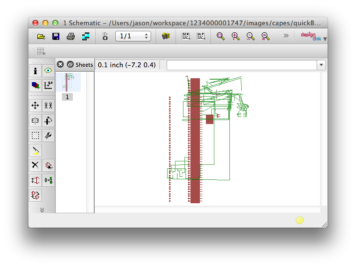
Fig. 268 Output of Upverter conversion
No one said it would be pretty!
I found that Eagle was more generous at reading in the +eaglexml+ format than the +eagle+ format. This also made it easier to hand-edit any translation issues.
Producing a Prototype
Problem
You have your PCB all designed. How do you get it made?
Solution
To make this recipe, you will need:
A completed design
Soldering iron
Oscilloscope
Multimeter
Your other components
Upload your design to OSH Park <http://oshpark.com> and order a few boards. The OSH Park QuickBot Cape shared project page shows a resulting shared project page for the quickBot cape created in Laying Out Your Cape PCB. We’ll proceed to break down how this design was uploaded and shared to enable ordering fabricated PCBs.

Fig. 269 The OSH Park QuickBot Cape shared project page
Within Fritzing, click the menu next to “Export for PCB” and choose “Extended Gerber,” as shown in Choosing “Extended Gerber” in Fritzing. You’ll need to choose a directory in which to save them and then compress them all into a Zip file. The WikiHow article on creating Zip files might be helpful if you aren’t very experienced at making these.
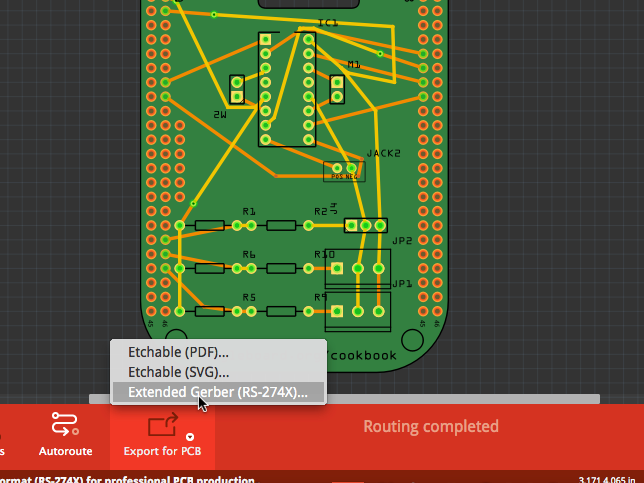
Fig. 270 Choosing “Extended Gerber” in Fritzing
Things on the OSH Park website are reasonably self-explanatory. You’ll need to create an account and upload the Zip file containing the Gerber files you created. If you are a cautious person, you might choose to examine the Gerber files with a Gerber file viewer first. The Fritzing fabrication FAQ offers several suggestions, including gerbv for Windows and Linux users.
When your upload is complete, you’ll be given a quote, shown images for review, and presented with options for accepting and ordering. After you have accepted the design, your list of accepted designs will also include the option of enabling sharing of your designs so that others can order a PCB, as well. If you are looking to make some money on your design, you’ll want to go another route, like the one described in Putting Your Cape Design into Production. QuickBot PCB shows the resulting PCB that arrives in the mail.
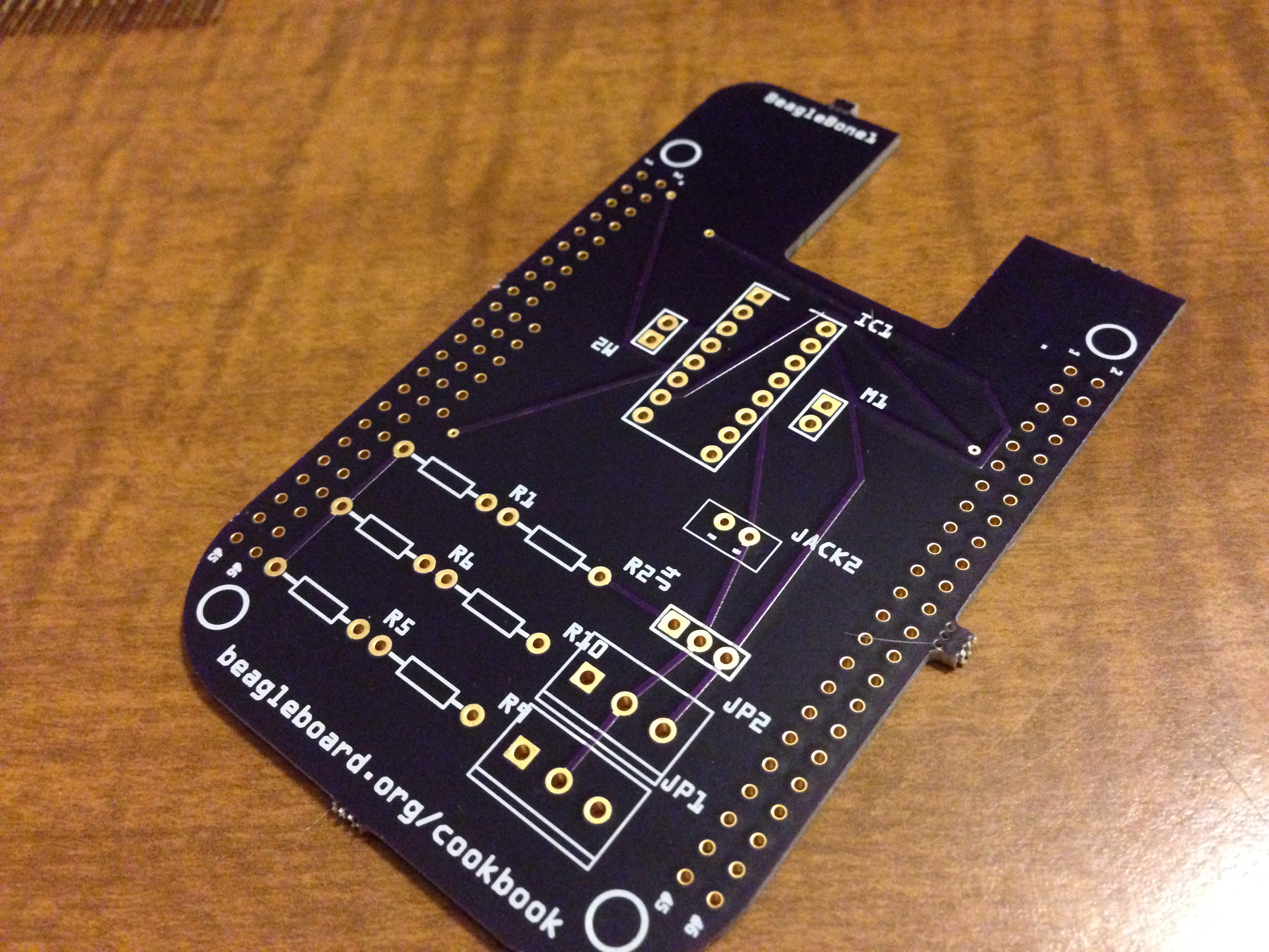
Fig. 271 QuickBot PCB
Now is a good time to ensure that you have all of your components and a soldering station set up as in Moving from a Breadboard to a Protoboard, as well as an oscilloscope, as used in Verifying Your Cape Design.
When you get your board, it is often informative to “buzz out” a few connections by using a multimeter. If you’ve never used a multimeter before, the SparkFun or Adafruit tutorials might be helpful. Set your meter to continuity testing mode and probe between points where the headers are and where they should be connecting to your components. This would be more difficult and less accurate after you solder down your components, so it is a good idea to keep a bare board around just for this purpose.
You’ll also want to examine your board mechanically before soldering parts down. You don’t want to waste components on a PCB that might need to be altered or replaced.
When you begin assembling your board, it is advisable to assemble it in functional subsections, if possible, to help narrow down any potential issues. QuickBot motors under test shows the motor portion wired up and running the test in Testing the quickBot motors interface (quickBot_motor_test.js).
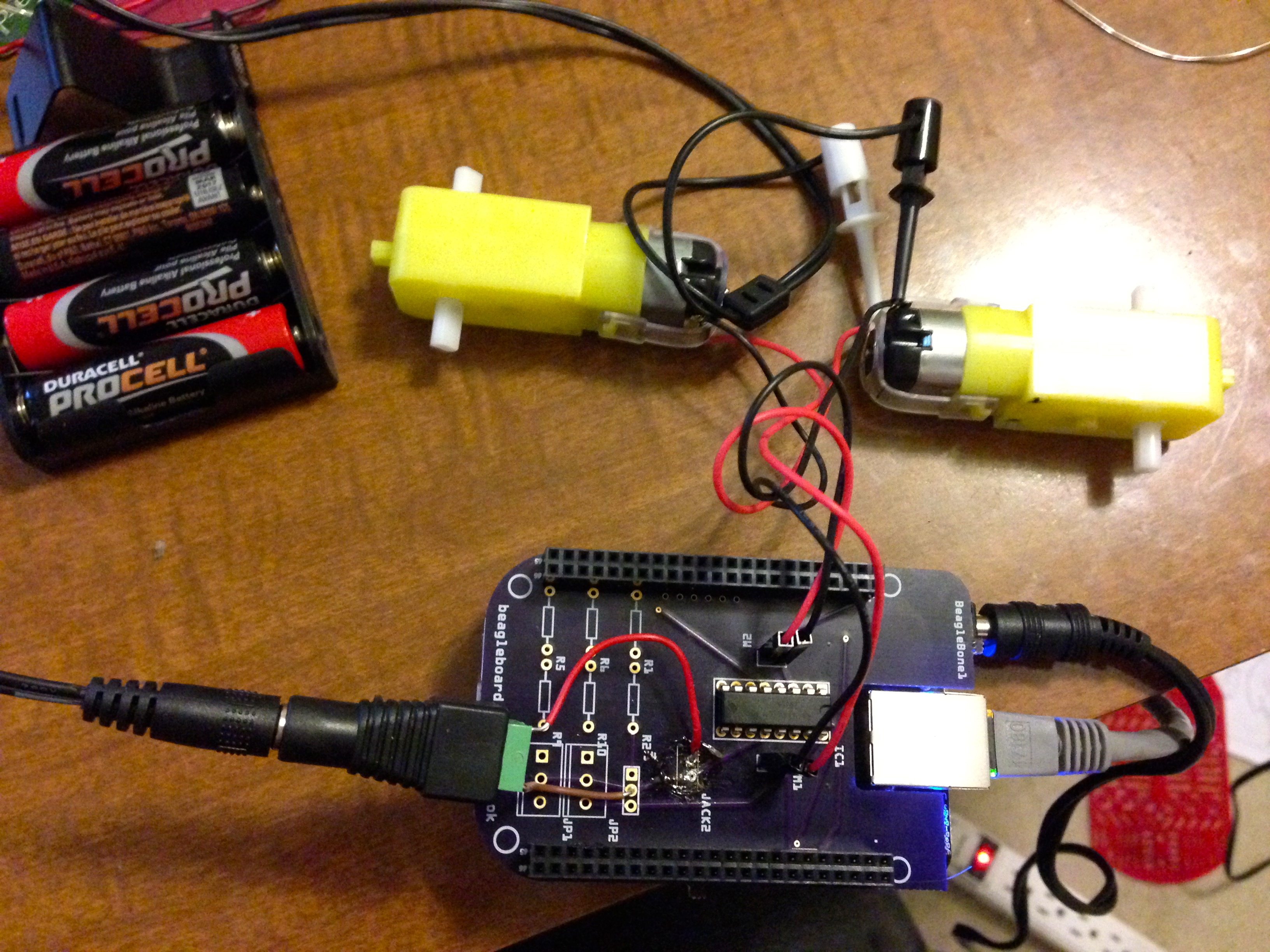
Fig. 272 QuickBot motors under test
Continue assembling and testing your board until you are happy. If you find issues, you might choose to cut traces and use point-to-point wiring to resolve your issues before placing an order for a new PCB. Better right the second time than the third!
Creating Contents for Your Cape Configuration EEPROM
Problem
Your cape is ready to go, and you want it to automatically initialize when the Bone boots up.
Solution
Complete capes have an I2C EEPROM on board that contains configuration information that is read at boot time. Adventures in BeagleBone Cape EEPROMs gives a helpful description of two methods for programming the EEPROM. How to Roll your own BeagleBone Capes is a good four-part series on creating a cape, including how to wire and program the EEPROM.
Putting Your Cape Design into Production
Problem
You want to share your cape with others. How do you scale up?
Solution
CircuitHub offers a great tool to get a quick quote on assembled PCBs. To make things simple, I downloaded the CircuitCo MiniDisplay Cape Eagle design materials and uploaded them to CircuitHub.
After the design is uploaded, you’ll need to review the parts to verify that CircuitHub has or can order the right ones. Find the parts in the catalog by changing the text in the search box and clicking the magnifying glass. When you’ve found a suitable match, select it to confirm its use in your design, as shown in CircuitHub part matching.
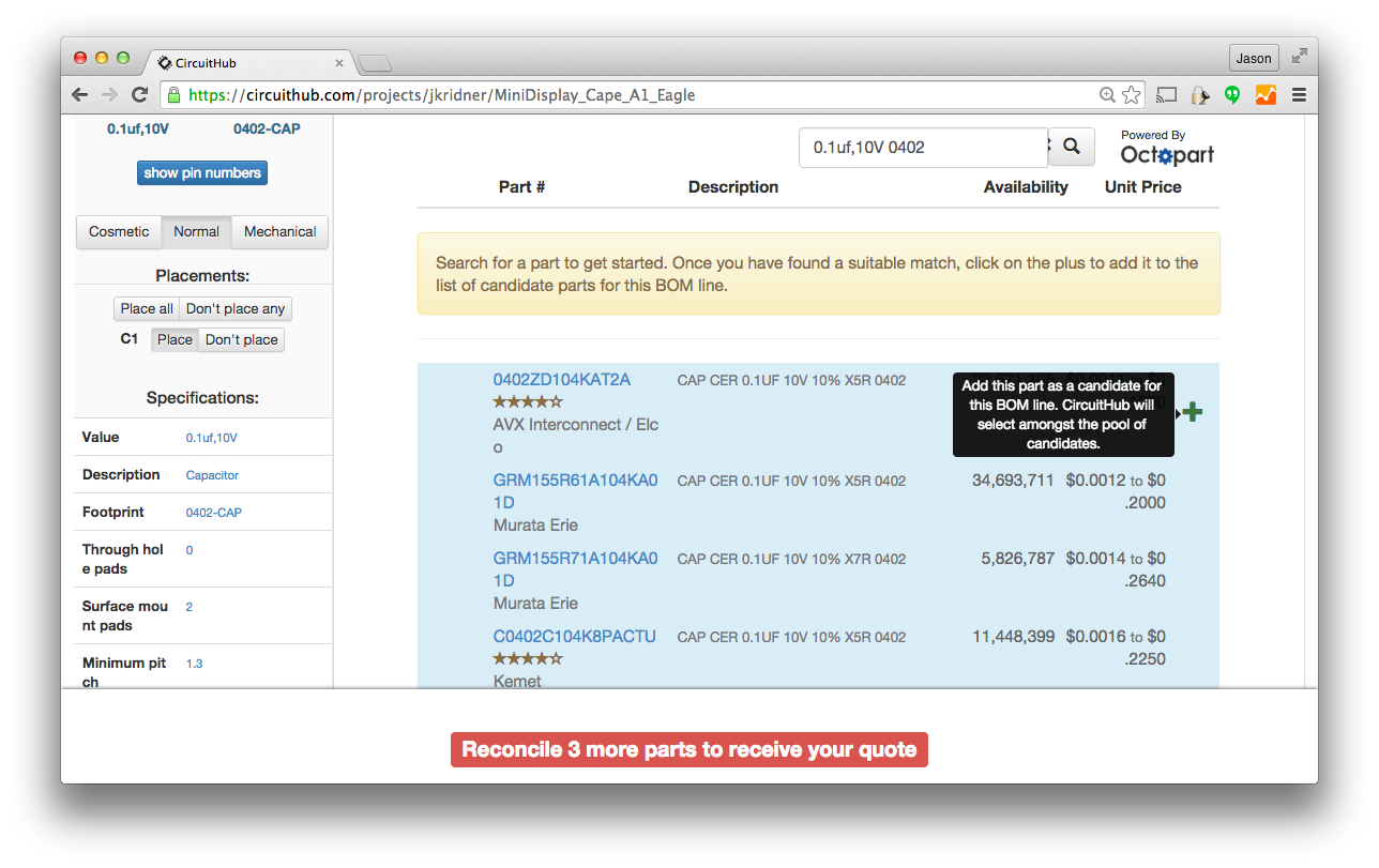
Fig. 273 CircuitHub part matching
When you’ve selected all of your parts, a quote tool appears at the bottom of the page, as shown in CircuitHub quote generation.
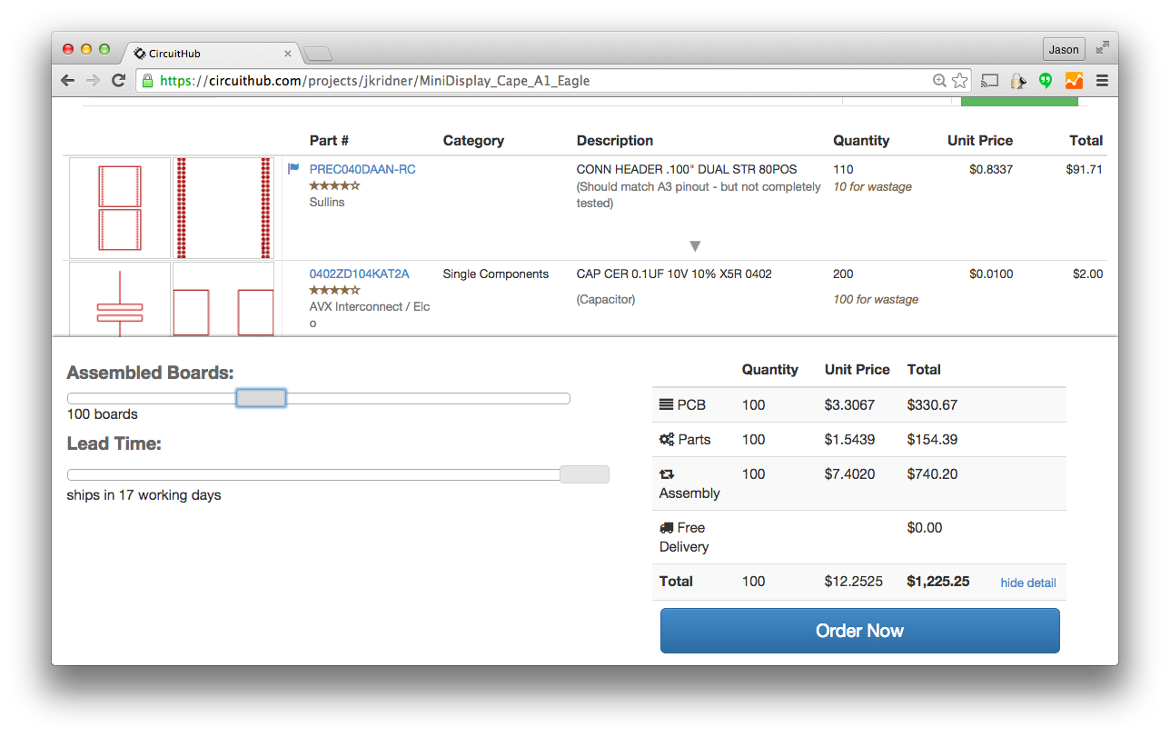
Fig. 274 CircuitHub quote generation
Checking out the pricing on the MiniDisplay Cape (without including the LCD itself) in CircuitHub price examples (all prices USD), you can get a quick idea of how increased volume can dramatically impact the per-unit costs.
Quantity |
1 |
10 |
100 |
1000 |
10,000 |
PCB |
$208.68 |
$21.75 |
$3.30 |
$0.98 |
$0.90 |
Parts |
$11.56 |
$2.55 |
$1.54 |
$1.01 |
$0.92 |
Assembly |
$249.84 |
$30.69 |
$7.40 |
$2.79 |
$2.32 |
Per unit |
$470.09 |
$54.99 |
$12.25 |
$4.79 |
$4.16 |
Total |
$470.09 |
$550.00 |
$1,225.25 |
$4,796.00 |
$41,665.79 |
Checking the Crystalfontz web page for the LCD, you can find the prices for the LCDs as well, as shown in LCD pricing (USD).
Quantity |
1 |
10 |
100 |
1000 |
10,000 |
Per unit |
$12.12 |
$7.30 |
$3.86 |
$2.84 |
$2.84 |
Total |
$12.12 |
$73.00 |
$386.00 |
$2,840.00 |
$28,400.00 |
To enable more cape developers to launch their designs to the market, CircuitHub has launched a http://campaign.circuithub.com[group buy campaign site]. You, as a cape developer, can choose how much markup you need to be paid for your work and launch the campaign to the public. Money is only collected if and when the desired target quantity is reached, so there’s no risk that the boards will cost too much to be affordable. This is a great way to cost-effectively launch your boards to market!
There’s no real substitute for getting to know your contract manufacturer, its capabilities, communication style, strengths, and weaknesses. Look around your town to see if anyone is doing this type of work and see if they’ll give you a tour.
Note
Don’t confuse CircuitHub and CircuitCo. CircuitCo is closed.